
- 11
- Nov
The situation of COVID-19 has not been fully controlled. The future housing and housing economy may become the norm.
The demand for semiconductors soared overnight, with a significant increase in the demand for sealing and testing.
In recent years, China’s chip design industry has maintained a high growth trend driven by factors such as improving self-sufficiency rate, upgrading of specifications and innovative applications with the support of policies..
Packaging testing is located in the middle and lower reaches of the semiconductor industry chain, including packaging and testing. Packaging is a series of processes such as dicing and pasting the fabricated wafer
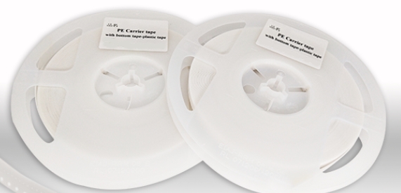
The carrier tape and upper cover tape are used to protect the chip on the wafer from damage caused by physical or chemical environmental factors and enhance the heat dissipation function of the chip
Advanced packaging technology has become one of the methods to continue Moore’s law, which drives the functional positioning of packaging in the electronic system to upgrade step by step.
Under the state’s preferential policies, abundant industrial funds and huge domestic demand, in the near future,
China’s semiconductor industry will be in the forefront of the world in more fields, which is of great concern value.